- 您现在的位置:买卖IC网 > Sheet目录345 > MT42L256M32D4KP-3 IT:A (Micron Technology Inc)IC LPDDR2 SDRAM 8GBIT 168FBGA
�� �
�
�2Gb:� x16,� x32� Mobile� LPDDR2� SDRAM� S4�
�Truth� Tables�
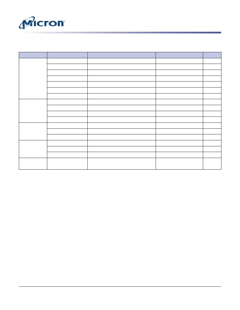
�Table� 51:� Current� State� Bank� n� to� Command� to� Bank� n� Truth� Table� (Continued)�
�Notes� 1–5� apply� to� all� parameters� and� conditions�
�Current� State�
�Idle�
�Row� active�
�Reading�
�Writing�
�Power-on�
�Resetting�
�Command�
�ACTIVATE�
�Refresh� (per� bank)�
�Refresh� (all� banks)�
�MRW�
�MRR�
�RESET�
�PRECHARGE�
�READ�
�WRITE�
�MRR�
�PRECHARGE�
�READ�
�WRITE�
�BST�
�WRITE�
�READ�
�BST�
�MRW� RESET�
�MRR�
�Operation�
�Select� and� activate� row�
�Begin� to� refresh�
�Begin� to� refresh�
�Load� value� to� mode� register�
�Read� value� from� mode� register�
�Begin� device� auto� initialization�
�Deactivate� row(s)� in� bank� or� banks�
�Select� column� and� start� read� burst�
�Select� column� and� start� write� burst�
�Read� value� from� mode� register�
�Deactivate� row(s)� in� bank� or� banks�
�Select� column� and� start� new� read� burst�
�Select� column� and� start� write� burst�
�Read� burst� terminate�
�Select column and start new write burst�
�Select� column� and� start� read� burst�
�Write� burst� terminate�
�Begin� device� auto� initialization�
�Read� value� from� mode� register�
�Next� State�
�Active�
�Refreshing� (per� bank)�
�Refreshing� (all� banks)�
�MR� writing�
�Idle,� MR� reading�
�Resetting�
�Precharging�
�Reading�
�Writing�
�Active� MR� reading�
�Precharging�
�Reading�
�Writing�
�Active�
�Writing�
�Reading�
�Active�
�Resetting�
�Resetting� MR� reading�
�Notes�
�6�
�7�
�7�
�7,� 8�
�9,� 10�
�9�
�11,� 12�
�11,� 12,� 13�
�14�
�11,� 12�
�11,� 12,� 15�
�14�
�7,� 9�
�Notes:�
�1.� Values� in� this� table� apply� when� both� CKE� n� -1� and� CKE� n� are� HIGH,� and� after� t� XSR� or� t� XP�
�has� been� met,� if� the� previous� state� was� power-down.�
�2.� All� states� and� sequences� not� shown� are� illegal� or� reserved.�
�3.� Current� state� definitions:�
�Idle:� The� bank� or� banks� have� been� precharged,� and� t� RP� has� been� met.�
�Active:� A� row� in� the� bank� has� been� activated,� and� t� RCD� has� been� met.� No� data� bursts� or�
�accesses� and� no� register� accesses� are� in� progress.�
�Reading:� A� READ� burst� has� been� initiated� with� auto� precharge� disabled� and� has� not� yet�
�terminated� or� been� terminated.�
�Writing:� A� WRITE� burst� has� been� initiated� with� auto� precharge� disabled� and� has� not� yet�
�terminated� or� been� terminated.�
�4.� The� states� listed� below� must� not� be� interrupted� by� a� command� issued� to� the� same� bank.�
�NOP� commands� or� supported� commands� to� the� other� bank� must� be� issued� on� any� clock�
�edge� occurring� during� these� states.� Supported� commands� to� the� other� banks� are� deter-�
�mined� by� that� bank’s� current� state,� and� the� definitions� given� in� Table� 52� (page� 109).�
�Precharge:� Starts� with� registration� of� a� PRECHARGE� command� and� ends� when� t� RP� is�
�met.� After� t� RP� is� met,� the� bank� is� in� the� idle� state.�
�Row� activate:� Starts� with� registration� of� an� ACTIVATE� command� and� ends� when� t� RCD� is�
�met.� After� t� RCD� is� met,� the� bank� is� in� the� active� state.�
�PDF:� 09005aef83f3f2eb�
�2gb_mobile_lpddr2_s4_g69a.pdf� –� Rev.� N� 3/12� EN�
�108�
�Micron� Technology,� Inc.� reserves� the� right� to� change� products� or� specifications� without� notice.�
�2010� Micron� Technology,� Inc.� All� rights� reserved.�
�发布紧急采购,3分钟左右您将得到回复。
相关PDF资料
MT45W1MW16BDGB-708 AT
IC PSRAM 16MBIT 104MHZ 54VFBGA
MT48H32M16LFB4-75B IT:C
IC SDRAM 512MB 54VFBGA
MT48H8M16LFB4-75 IT:K TR
IC SDRAM 128MBIT 133MHZ 54VFBGA
MTC100-JA2-P34
CONTACT INSERT PIN
MX841BE
IC CONVERTER WHITE LED 8-SOIC
MXHV9910BTR
IC LED DRIVER HIGH BRIGHT 8-SOIC
MXN12FB12F
MOTOR BRUSHED DC 12V 2922RPM
MXN13FB08B1
MOTOR BRUSHED DC 8V 4714RPM
相关代理商/技术参数
MT42L256M32D4KP-MS
制造商:Micron Technology Inc 功能描述:256MX32 LPDDR2 PLASTIC IND TEMP GREEN WFBGA 1.2V - Bulk